
Riteshkumar Bhojani1, Jens Kowalsky1, Josef Lutz1, Dustin Kendig2, Roman Baburske3, Hans-Joachim Schulze3, Franz-Josef Niedernostheide3
Email: riteshkumar.bhojani@etit.tu-chemnitz.de
1Chair of Power Electronics and EMC, Technische Universität Chemnitz, Chemnitz, Germany
2Microsanj, Santa Clara, USA
3Infineon Technologies AG, Neubiberg, Germany
摘要:在本文中,我们首次通过实验测量了igbt中重复短路(SC)事件下的current filaments现象。这些current filaments现象是通过反射率热成像系统 (TRM)发现的。对两种不同焊接方式的15A-1200V IGBT芯片进行了破坏电流的测定。重复的 SC 事件与 TRM 测量相结合,表明在不同 VCE 下存在大范围的非破坏性current filaments现象。在支持基于多单元 IGBT 结构的 TCAD 器件模拟中,观察到短路条件下类似的现象形成。他们具有与 TRM 测量的当前current filaments现象相似的尺寸。
关键词—IGBT,短路,电流丝,反射率热成像系统
Ⅰ
INTRODUCTION
In previous works, several authors have shown short-circuit destruction limits and the improvement potential of the SC- SOA for IGBTs of different voltage classes with a minimum current destruction limit at about 50 % of the rated voltage [1- 4]. These observations were linked to the effect of current crowding at the collector side of the IGBT. Moreover, different failure modes like failure during the SC pulse and during SC turn-off were also related with the current crowding effect in IGBTs. Up to now, direct experimental evidence for the appearance of the current filaments in IGBTs during short- circuit is missing.
In this work, we investigated the behavior of the current filaments using CCD-based thermo-reflectance microscopy [5]. Under different voltage and current conditions, thermo-reflectance measurements were performed to observe the change in temperature on the top of the IGBT metallization.
Ⅱ
THERMO-REFLECTANCE MICROSCOPY
In general, the complex refractive index of a material changes with temperature, and the thermo-reflectance coefficient Cth simply represents the linear change in optical reflectance of a surface due to a change in temperature (ΔT) [5]:
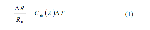
Here, Cth is the thermo-reflectance coefficient, R is the reflective intensity in (J/m2), T is the temperature in (K) and λ is the wavelength in (m).
The stroboscopic imaging was used to create time-resolved image data with temporal resolution down to 50 ns. The device is turned ON for a certain period of time at a certain duty cycle, and the CCD exposure time is also set by the user as shown in Fig. 1(a). Nearly all the light reaching the CCD will come from the LED pulses which are offset by a specific time delay relative to the device excitation, and a CCD image is generated as the sum of the LED pulses inside a single CCD exposure window. The timing diagram in Fig. 1(a) shows how the time-resolved image data is collected by pulsing the device excitation and LED probe light with a controllable relative time delay.
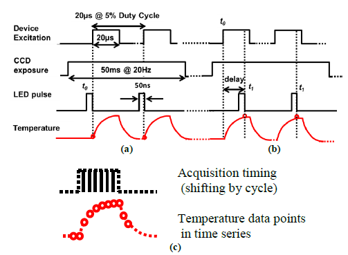
Fig. 1(a) Timing diagram showing how the t = 0 data point is collected (b) Timing diagram showing how the t > 0 data point is collected for heated device (c) Acquired temperature data points with respect to time.
Fig. 1(b) and (c) show how the temperature data points were acquired by shifting the time delay after each cycle to achieve time resolution, limited only by how tightly the pulse of the LED probe light was set. To create a two-dimensional transient thermo-reflectance image, a reference CCD image with LED pulse delay t = 0 was collected, followed by recording a CCD image at t > 0. Then, a sub-pixel image registration algorithm was applied to a subset of the CCD images to align the t > 0 image to the reference. After this, the registered t > 0 images were subtracted from the t = 0 reference image. This process with recording pairs of t = 0, t > 0 images was continued as a running average to suppress noise to an acceptable level. In this way, the software automatically stepped through user-designated time delays and averaging times to collect a full time-domain image set, from the moment the device was turned on, to the time period after the device switched off and was cooling down.
Ⅲ
SC THEORY AND FILAMENT BEHAVIOR
A.Simulation results of current filaments during SC
Electro-thermal device simulations were performed to estimate the surface temperature during the SC pulse when current filaments are present in the chip. Fig. 2 shows the transients of the maximum and the average current density together with the course of the maximum temperature under SC conditions for a DC-link voltage VDC = 500 V, a collector current IC = 240 A, corresponding to a gate-emitter voltage VGE = 30 V at an initial temperature Tint = 300 K for a multi- cell IGBT structure with a simplified front side structure [4]. The thermal resistance of 3.2 K/W was set at the collector contact and self-heating was considered for SC simulations.
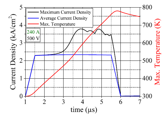
Fig. 2. Transients of the maximum and the average current density and the transient of the maximum temperature from electro-thermal SC simulation at VDC = 500 V, IC = 240 A, Tint = 300 K.
A small window at n–base/n-field-stop junction (Fig. 3) was selected to extract the average and maximum current densities from the device. At 2.5 µs, the two current density transients start to split. At 4 µs, multiple filaments are present in the device (Fig. 3). The typical width of the filament at the emitter-side metallization was between 80 to 120 µm.
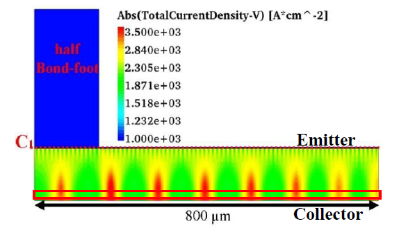
Fig. 3. Current density distribution at 4 µs in IGBT with ref. to Fig. 2.
Fig. 4 shows the surface temperature profile with respect to a horizontal cut C1 in Fig. 3 on top of the Al metallization. At the filament positions, where the simulated temperature close to the collector is about 600 K at 4 µs, the surface temperature shows an increase by 2 to 5 K, which can be resolved using TRM.
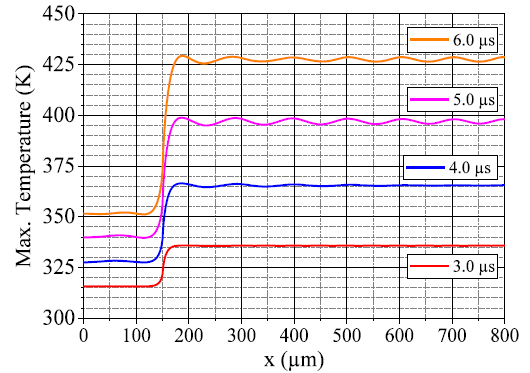
Fig. 4. Surface temperature profile on top of the Al metallization at different time points from Fig. 2.
B.Low Inductive Short-circuit Setup
Fig. 5(left) displays the SC-setup combined with thermo- reflectance microscopy setup. Fig. 5(right) shows a close view of a SC-setup including capacitor bank, measuring probes, TRM lens and a Device Under Test (DUT). The DUT is soldered on a Direct Copper Bonding (DCB) substrate.
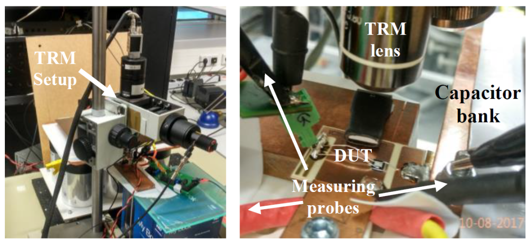
Fig. 5. A SC-setup with TRM camera setup (left) and an experimental setup of TRM lens with a low inductive SC-setup (right).
A very low inductive (Lpar ≤ 60 nH) short-circuit setup was designed to investigate the current destruction limit for the 15 A-1200 V IGBTs. The short-circuit destruction limit was measured for two differently wire-bonded IGBT chips shown in Fig. 6. The gate resistors for turn-on and turn-off were set to RG = 220 Ω during all measurements.
The results shown in Fig. 6 indicate that the critical short- circuit current is independent of the number of bond wires on the top of aluminum metallization, allowing us to use chips with only one bond wire for TRM. The temperature on the top surface of the IGBT chip was continuously monitored using a “Microsanj NT210 transient thermo-reflectance camera” by performing repetitive non-destructive SC events. Fig. 7 shows a SC type-1 waveform at VDC = 400 V and VGE = 30 V. An estimated average temperature swing ΔTSC of the chip during this given pulse can be about 67 K using the whole chip volume given by Equation 2 in [6].
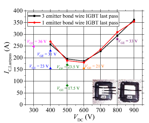
Fig. 6. Destruction limit of 1.2 kV IGBTs for two differently wire-bonded chips at T = 300 K, Lpar ≤ 60 nH, RG = 220 Ω (red and black points) and SC measurement conditions at which non-destructive filaments were investigated by means of TRM (scattered points).
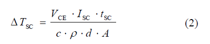
where c is the specific heat capacity of silicon, r is the density of silicon, d and A are thickness and area of the chip.
With TRM, the uncovered Al surface was monitored for different VDC by performing repetitive SC events close below the destruction limit. The measurements were performed for gate voltages close to the chip destruction as well as for reduced gate voltages. The SC pulse length was set to 4 µs. The time between each consecutive SC pulse was set to 200 ms which was sufficient to cool down the IGBT top aluminum metallization. The scattered points in Fig. 6 refer to measurement conditions of the IGBT chips at which TRM measurements were performed with different VDC, VGE and IC.
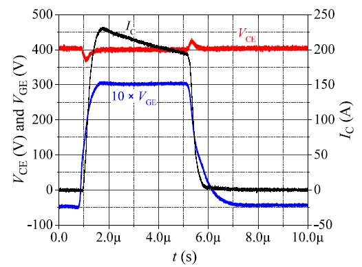
Fig. 7. Transients of the VCE(t), VGE(t) and IC(t) for a SC type-1 event at VCE = 400 V, VGE = 30 V, T = 300 K, Lpar = 60 nH and RG = 220 Ω.
C.Destructive and non-destructive filaments
Fig. 8 schematically illustrates the areas in the IC-VCE phase space in which either no filaments or non-destructive filaments were observed by TRM. The red-solid line marks the dependency of the destruction current on VCE under SC conditions with the minimum critical SC current lying at about VCE,rated/2 for the investigated 1200 V IGBTs. The green line explicates the current level above which filament appears. The hatched area in Fig. 8 between the red-solid and the green- dashed line covers the non-destructive visible filaments, especially at a low VCE range from 300 V to 600 V. The filament pattern becomes finer from VCE of 300 V to 600 V. For VCE > 600 V, the filament behavior needs to be inquire further. In the area below the green-dashed line, current crowding did not appear and the current flowed uniformly in the IGBT during SC event. The black line indicates the IC-VCE characteristic for VGE ≤ 15 V. For the safe operation of the IGBT device during SC case, it is essential to evaluate this green-dashed boundary line. Therefore, the focus of the TRM was different gate voltages at which the uniform current distribution transformed into a distribution with current filaments, indicated by green-dashed line in Fig. 8, especially at low VCE voltages.
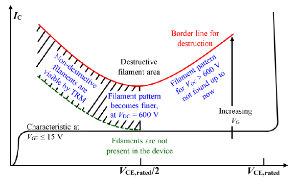
Fig. 8. Schematic illustration of the border lines for destructive and non- destructive filament areas in IC-VCE phase space.
Ⅳ
TRM RESULTS AND DISCUSSION
Fig. 9 displays the TRM images at different DC-link voltages and different gate voltages. At VDC = 400 V and VGE of 30 V (Fig. 9a), after integration over several thousand SC pulses, temperature peaks are visible for the IGBT chip with one emitter bond wire. The TRM images show the temperature difference (ΔT), between t = 0 and t > 0 images, and not the actual temperature. The blue color indicates the coldest region on the IGBT chip. The red spots show high temperature areas indicating filaments in the IGBT. They have similar dimensions as the filaments found in simulation (Fig. 3). The diameter of the current filaments ranges from minimum 40 µm to maximum 140 µm. Their distance varies from 50 µm to 200 µm. The different maximum temperatures at the position of the current filaments indicate that the filaments were carrying different currents. For certain conditions also clustering of filaments was observed.
For VDC/VGE = 300 V/36 V, 400 V/23 V and 500 V/17.5 V (Fig. 9c-e) again the filaments appeared. For VDC = 400 V and 500 V, the gate voltage is 12 V and 7 V lower that the critical gate voltage at which destruction occurs, indicating a wide gate voltage and collector current interval at which non-destructive filaments may appear. The filament pattern was almost regular for VDC = 400 V (Fig. 9d). However, there is a gradient of the maximum filament temperature from the left to the right edge of the TRM image.
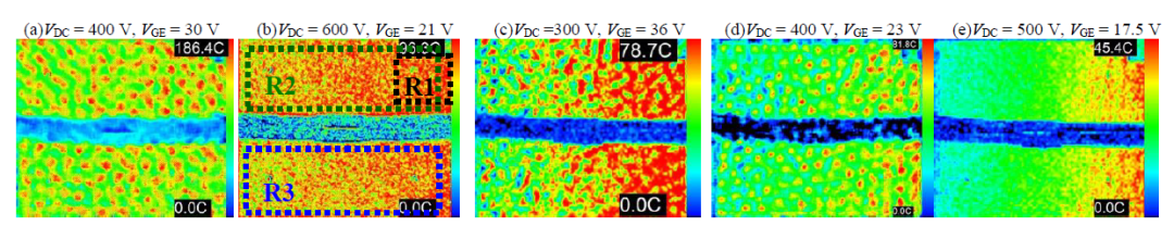
Fig. 9. Surface temperature observation after series of SC pulses using TRM camera at different VDC and VGE. (Scale: temperature difference to coldest point (x: 3.7 mm, y: 2.8 mm))
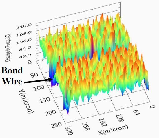
Fig. 10. 3D-TRM image after SC events at VDC = 400 V (ref. to Fig. 9(a), Scale: 0.1× (X, Y)).
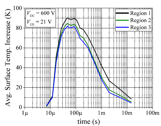
Fig. 11. Measured average surface temperature profile on top of the Al metallization from three different regions with respect to time.
Fig. 10 shows the 3D-TRM picture of the temperature profile with respect to Fig. 9(a) at VDC =400 V. Fig. 11 shows the measured average surface temperature profile on top of aluminum metallization from three different regions with respect to time after repetitive SC events. These three different regions R1, R2 and R3 were selected from Fig. 9(b) after several repetition of the short-circuit events at VDC = 600 V and VGE = 21 V. Since the heat inside the chip takes some time to reach the top metallization, one can initially see a very small increase in temperature. After 50 µs, the temperature on the chip surface reaches the maximum value and remains the same for another 50 µs. From 100 µs, the temperature of the aluminum metallization starts to decay. Several 10 milli- seconds after the SC pulse, the Al surface metallization reaches its initial temperature.
Ⅴ
CONCLUSION
Current filaments were observed in IGBTs during repetitive SC events using thermo reflectance microscopy. The diameters of the filaments varied between 40 µm and 140 µm and were comparable to the width of filaments (80 µm to 120 µm) found in supporting TCAD device simulations. The filaments were more pronounced for low DC-link voltages (300 V to 600 V), while at higher DC-link voltages, the filament pattern became finer and transformed to a homogeneous distribution. The filaments were also found at gate voltages lower than the critical gate voltages. The measured results indicate that there is a wide current range where the non-destructive filaments can appear inside the IGBT device during repetitive SC events. In all measurements, irregular patterns of filaments were observed. However, the filaments showed characteristic dimensions and were spaced apart from each other by characteristic distances.

ACKNOWLEDGEMENT
The authors would like to thank Madhu Lakshman Mysore for his help during the measurement and also to Manuela Schulze for critically reading the manuscript.